

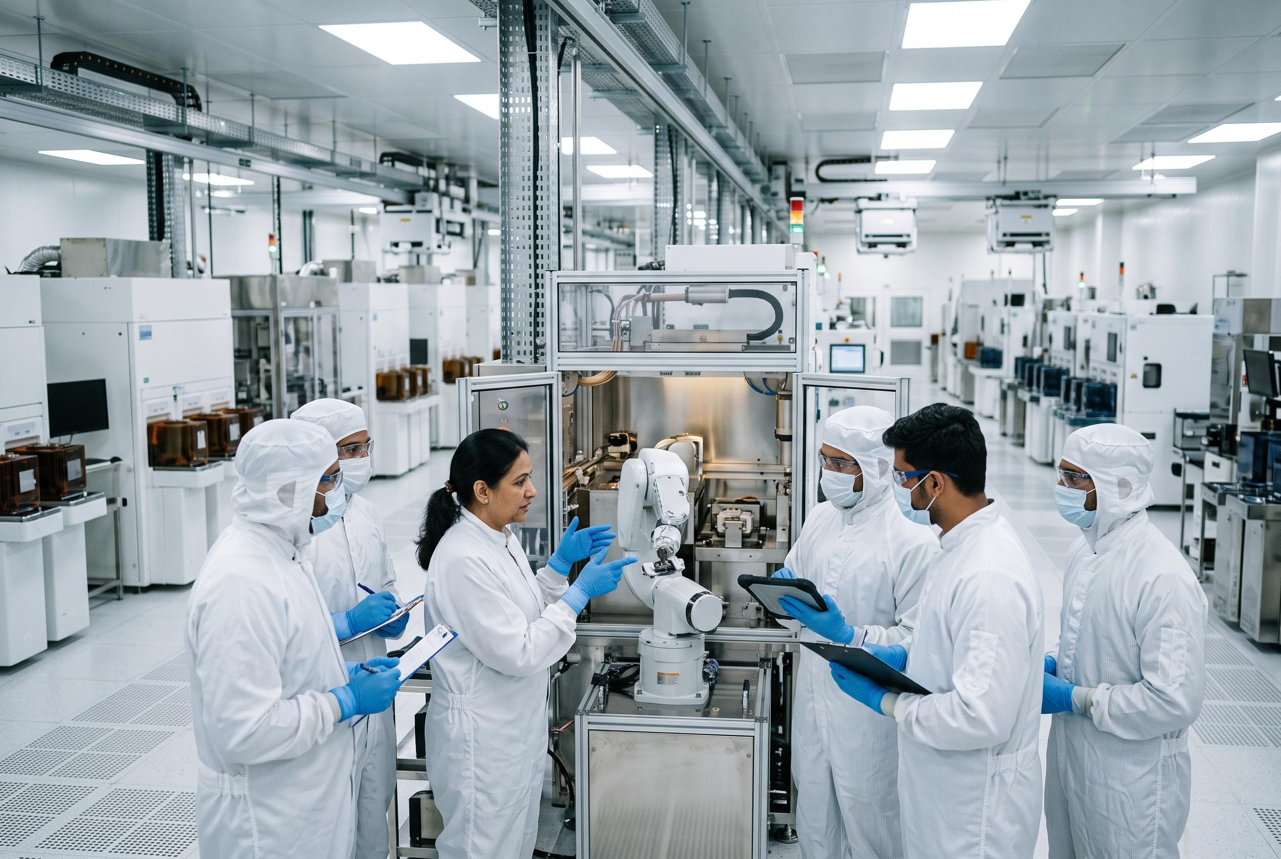

India accelerates its semiconductor ambitions with ambitious policy measures, international collaborations, and a focus on design talent, signalling a move from promises to tangible industrial hardware development.
India has moved from pledges to rule-making in its chip drive, issuing notifications on 31 August for all six pillars of Semicon 2.0 after the Union Cabinet approved the scheme in July with an outlay of Rs 1,27,500 crore, or roughly $13 billion. Officials say the programme is meant to support everything from chip design and wafer fabrication to packaging, equipment, materials, research and talent, while reporting in the South China Morning Post has framed the effort as an attempt to turn “Make in India” into “Engineer in India”. (pib.gov.in) The message from New Delhi is that semiconductors are no longer being sold as a single showcase factory, but as a long industrial build-out.
That broader pitch rests on a first phase which the government says has already approved 12 manufacturing units across six states with cumulative investment of more than Rs 1.64 lakh crore. According to the Prime Minister’s Office and the Press Information Bureau, the approved slate includes one silicon fab, one silicon carbide fab, one gallium nitride micro LED display fab and nine packaging units, with Micron, Kaynes and CG Semi already in commercial production. (pmindia.gov.in) The South China Morning Post noted that the first phase was largely about foundational industrial set-up, and that India is making its move as Japan and Singapore, among others, also spend heavily on chips after the pandemic-era shortages exposed the risks of relying on a narrow cluster of East Asian manufacturing centres. (scmp.com)
The strongest part of India’s argument may be labour rather than lithography. Government figures released in July said the country accounts for nearly 20% of the world’s semiconductor design talent, while the Chips to Startup programme has deployed design tools in 320 academic institutions and trained more than 68,000 students; a new semiconductor curriculum has also been adopted by more than 500 engineering colleges. (pib.gov.in) In the 31 August briefing on the scheme, electronics minister Ashwini Vaishnaw said India had already met its target of developing 85,000 semiconductor engineers in four years, far earlier than planned, and had now set itself a fresh goal of training another 100,000. (pib.gov.in) That helps explain why the official language around Semicon 2.0 leans so heavily towards design, R&D and manpower rather than factories alone.
At the centre of the manufacturing push sits Tata Electronics’ project at Dholera in Gujarat, but official timelines show that the most difficult stage still lies ahead. The Prime Minister’s Office said in July that India’s first fab is scheduled to be commissioned in 2028, even as the government continues to present Dholera as the country’s first front-end semiconductor facility, the part of the chain where wafers are actually made before chips move on to packaging and testing. (pmindia.gov.in) A Commerce Ministry notification issued in April said the special economic zone for Tata Semiconductor Manufacturing would cover 66.166 hectares and was expected to provide employment for 21,000 people. (pib.gov.in) The scale underlines the size of India’s wager, but also the length of the runway.
The international anchor for that wager is ASML, the Dutch group whose lithography machines are central to modern chipmaking. Reuters reported in May that Tata Electronics and ASML signed their agreement in the presence of Narendra Modi and Dutch prime minister Rob Jetten, with ASML’s technology backing Tata’s planned 300-millimetre fab in Dholera and Tata putting $11 billion into the project. (indianexpress.com) News9 said the partnership was designed not only to equip the fab but also to support local talent training, lithography skills, research infrastructure and supply-chain resilience. (news9live.com) ASML chief executive Christophe Fouquet said: “India’s rapidly expanding semiconductor sector represents many compelling opportunities, and we are committed to establishing long-term partnerships in the region.” (indianexpress.com)
Technical details emerging around Dholera suggest India is starting with commercially important, older-generation chipmaking rather than attempting the most advanced nodes at the outset. EE Times reported that the site is designed for capacity of 50,000 wafers a month and is expected to make high-performance logic chips, radio-frequency-enabled systems on chip for Bluetooth and Wi-Fi, Internet of Things products, power-management integrated circuits, display drivers and non-volatile memory devices. (eetimes.com) News9 reported that Tata’s access to process technologies through its partnerships spans 28nm, 40nm, 55nm, 90nm and 110nm, while EE Times said construction is under way on a 160-acre site with about 1,500 workers engaged and that Tata has also tied up with Taiwan’s PSMC, Tokyo Electron and Synopsys. (news9live.com) That is a pragmatic industrial strategy: begin where demand is broad and execution risks are lower, then try to climb.
What gives the Dutch link added weight is that it goes well beyond one factory. In a joint statement issued by The Hague and New Delhi, the two governments said they welcomed a framework for deeper cooperation in semiconductors covering investment, research and talent exchange, alongside plans to connect the Dutch Semicon Competence Centre with the Indian Semiconductor Mission. (government.nl) The same statement set out a “brain bridge” between Eindhoven University of Technology, the University of Twente and six Indian institutes – IISc Bangalore, IIT Bombay, IIT Delhi, IIT Gandhinagar, IIT Guwahati and IIT Madras – with industry participation from NXP, ASML, TATA and CG Semi. (government.nl) That makes the India-Netherlands relationship look less like a one-off equipment deal and more like a long-term attempt to build an ecosystem around skills and research.
The next public test comes later this month. SEMI and the India Semiconductor Mission say SEMICON India 2026 will run in New Delhi from 17 to 19 September, with organisers presenting it as evidence that India is moving from attracting investment to building a fully integrated semiconductor ecosystem. (semi.org) Whether that ambition is met will depend on more than subsidy announcements: India has shown it can bring packaging lines into production, but the harder task is to convert design talent, foreign partnerships and state support into dependable fabrication capacity on a timetable the industry will trust. The direction of travel is now clearer than it was a year ago.
Disclaimer: This article is intended to inform and educate, not to recommend or endorse any financial product, investment or strategy. Please consider your own financial circumstances and seek professional advice where appropriate before making financial decisions.