

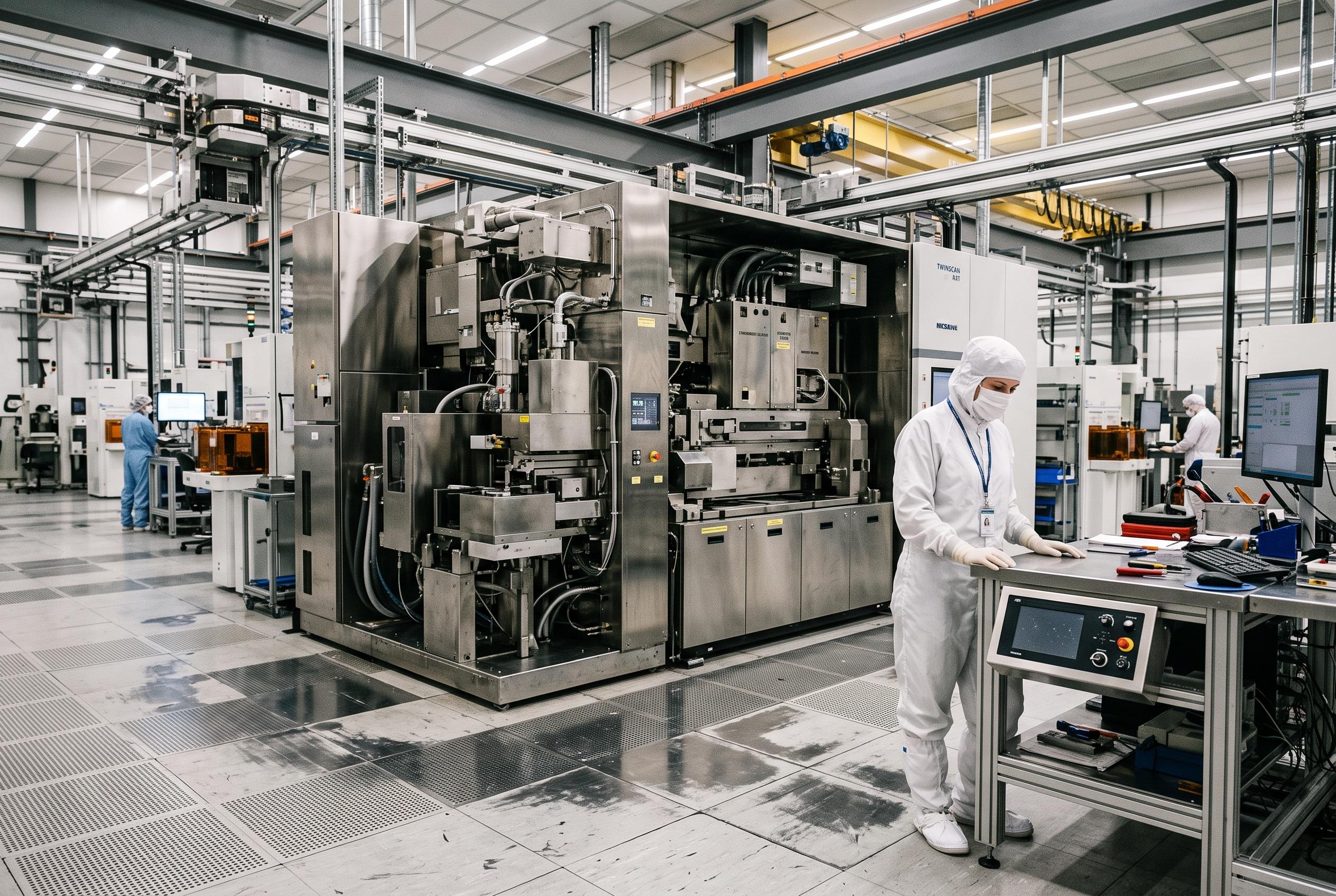

India’s push to establish a domestic semiconductor fabrication sector is finally taking shape, with flagship projects like Tata’s ₹91,000 crore chip fab signalling a new era of deep investment and strategic industry-building, despite the sector’s capital-intensive nature and long-term horizon.
India’s drive to build a domestic semiconductor fabrication base is moving from policy ambition to industrial reality. The sector remains extraordinarily capital-intensive, but it also sits at the intersection of national strategy, supply-chain security and import substitution. According to India Briefing, the India Semiconductor Mission is providing fiscal support for fabs, compound-semiconductor units and assembly-and-test facilities, with government backing reaching as much as 50% of project costs under various schemes. That policy push has helped lift the industry from theory into execution, with 13 semiconductor projects approved across seven states as of 18 May 2026.
The scale of the opportunity is matched by the scale of the investment. Semiconductor fabrication plants vary sharply in cost depending on whether the project is an assembly, test and packaging unit, a compound-semiconductor facility or a leading-edge wafer fab. In broad terms, entry-level back-end projects can require a few hundred crore rupees, while advanced silicon fabs can run into tens of thousands of crore. The Economic Times reported that India’s first chip fab, a Tata Semiconductor Manufacturing project in Dholera, Gujarat, has been notified as a special economic zone and involves an investment of ₹91,000 crore, underlining how large the current wave of projects has become.
That investment is being backed by a growing ecosystem of technology partners and equipment suppliers. Tom’s Hardware reported that ASML is working with Tata Electronics on India’s first commercial semiconductor fab in Dholera, with Taiwanese partner Powerchip Semiconductor Manufacturing Corporation also involved in design and construction support. The project is expected to produce chips in the 110nm to 28nm range, with a target capacity of 50,000 wafers a month, aimed at markets including automotive, mobile, AI and communications. Those details point to the way India is entering the industry: first through focused, commercially viable nodes rather than the most advanced frontier technologies.
Behind the headline projects, the economics of chip manufacturing remain unforgiving. IMARC Group says process equipment typically accounts for the largest share of capital spending, while cleanrooms, ultra-pure water systems, power infrastructure and environmental controls also absorb substantial outlay. Operating costs are driven by materials, chemicals, power and highly skilled labour, and profitability depends heavily on yield, the proportion of wafers that come out functional. IMARC estimates payback periods of 7 to 12 years, which makes this a long-horizon industrial bet rather than a conventional manufacturing play.
Location choice is equally important. Site selection is shaped by water security, uninterrupted power, vibration-free construction, access to engineering talent and the availability of state incentives. IMARC identifies Gujarat, Assam, Karnataka, Uttar Pradesh, Tamil Nadu and Telangana as leading contenders, reflecting both industrial depth and policy support. The company’s project guidance also stresses that a fab requires a wide range of approvals, including factory licensing, pollution-control consents, hazardous-material authorisation, environmental clearances and fire and chemical safety sign-off, all of which must be handled early if a project is to move on schedule.
For investors, the key lesson is that semiconductor fabrication in India is less a single project than a staged industrial system. IMARC’s project guidance suggests many entrants will find the best risk-adjusted route through assembly, test and packaging or compound-semiconductor facilities before considering more complex wafer fabs. India Briefing’s account of the incentive structure, along with the wave of approved projects and technology partnerships, suggests the environment is now materially more supportive than it was even a year ago. But the business still demands patient capital, robust partnerships and disciplined execution, because in semiconductors, delay and yield loss are costly in a way few other industries can match.
Disclaimer: This article is intended to inform and educate, not to recommend or endorse any financial product, investment or strategy. Please consider your own financial circumstances and seek professional advice where appropriate before making financial decisions.