

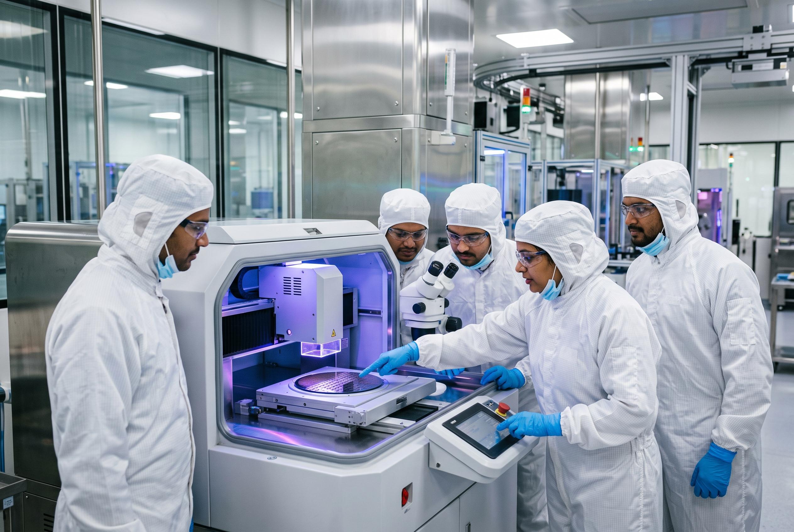

India is shifting its semiconductor ambitions towards specialised manufacturing and advanced packaging, leveraging foreign partnerships and targeted investments to build a resilient, high-value ecosystem rather than competing in every segment of chip production.
India’s semiconductor push is becoming more selective, and more ambitious, than a simple race to copy the world’s biggest chipmaking powers. A May roadmap from NITI Aayog argues that India should stop trying to do every part of the business at once and instead build depth where it can move fastest, especially in chip design, advanced packaging and compound semiconductors. The urgency is clear enough: the same policy work says roughly 90-95% of India’s current semiconductor demand is still met through imports, even as the domestic market is projected to climb from about $90bn by FY30 to nearly $200bn by FY35.
That strategic rethink is now being paired with high-profile industrial tie-ups. On 16 May in The Hague, Narendra Modi and Dutch Prime Minister Rob Jetten witnessed Tata Electronics and ASML sign an agreement linked to the Dholera project in Gujarat, which the Indian government described as the country’s first front-end semiconductor fab. ASML said the partnership would help establish and ramp Tata’s 300 mm plant by supplying lithography tools and by working on research infrastructure, supply-chain resilience and local skills.
For Tata, the arrangement is not just an equipment order. ASML said the Dholera fab carries a planned investment of $11bn and is intended to supply chips for automotive, mobile and artificial intelligence uses to customers around the world. Tata’s own account adds that, through its wider partnership with Taiwan’s PSMC, it has access to a technology portfolio spanning 28nm, 40nm, 55nm, 90nm and 110nm. That range matters because it suggests India is beginning with mature and speciality nodes that still have large commercial markets, rather than trying to vault straight into the most advanced end of the industry.
That is broadly the course laid out by NITI Aayog. Its roadmap says India should choose “leadership and purpose over participation” and shift towards the “More-than-Moore” phase of chipmaking, where advanced packaging, system integration and manufacturing scale can matter as much as chasing the smallest transistor sizes. By 2035, it says, India should aim to build a semiconductor value chain worth $120bn-$150bn and establish itself among the world’s top three destinations for outsourced semiconductor assembly and test, or OSAT, as well as advanced packaging.
The harder question is who pays. Reporting on the roadmap, NDTV Profit said India may need $135bn-$180bn of investment over the next decade to assemble a globally competitive semiconductor ecosystem, with the government expected to fund at least one-third in order to de-risk projects and draw in private capital. The same reporting said NITI Aayog wants large semiconductor manufacturing zones with standardised governance and dependable utilities. Business Standard’s reading of the report points in the same direction: this is not a plan for isolated factories, but for an industrial platform that can support suppliers, materials, packaging and specialised production at scale.
Executives and officials alike have stressed that the ecosystem will not be built by concrete and machines alone. ASML said its work with Tata would include domestic talent, supply chain and research initiatives intended to support the fab over the long term, while Tata framed the Dutch company’s lithography systems as part of a wider network of equipment, process, design technology and materials partnerships. Randhir Thakur, Tata Electronics’ chief executive, said ASML’s expertise would help ensure the “timely ramp” of the Dholera fab and create a “resilient and trusted supply chain”. Christophe Fouquet, ASML’s chief executive, said India’s semiconductor sector presented “many compelling opportunities”.
Even so, the real test may begin after production starts. Business Standard noted that Indian-made chips will have to meet exacting global standards on performance and reliability before buyers treat them as credible alternatives in a highly specialised supply chain. The NITI roadmap makes a similar point in more strategic terms: India should not simply chase the wafer-fab race from behind. Its preferred near-term emphasis is on mature-node logic, speciality analogue and mixed-signal devices, and materials such as silicon carbide and gallium nitride, which are increasingly important in power electronics, mobility and other strategic applications.
The wider wager is that India can use its existing design strength to climb into higher-value manufacturing and packaging before its import dependence becomes even more expensive. If policymakers can combine public support, industrial zones, foreign technology partnerships and a strong domestic skills base, India may not need to dominate every layer of semiconductor production to become important to the global market. The goal set out across government and industry documents is narrower than a full imitation of Taiwan or the United States, but potentially more realistic: to become indispensable in selected parts of the chip business rather than merely present in it.
Disclaimer: This article is intended to inform and educate, not to recommend or endorse any financial product, investment or strategy. Please consider your own financial circumstances and seek professional advice where appropriate before making financial decisions.