

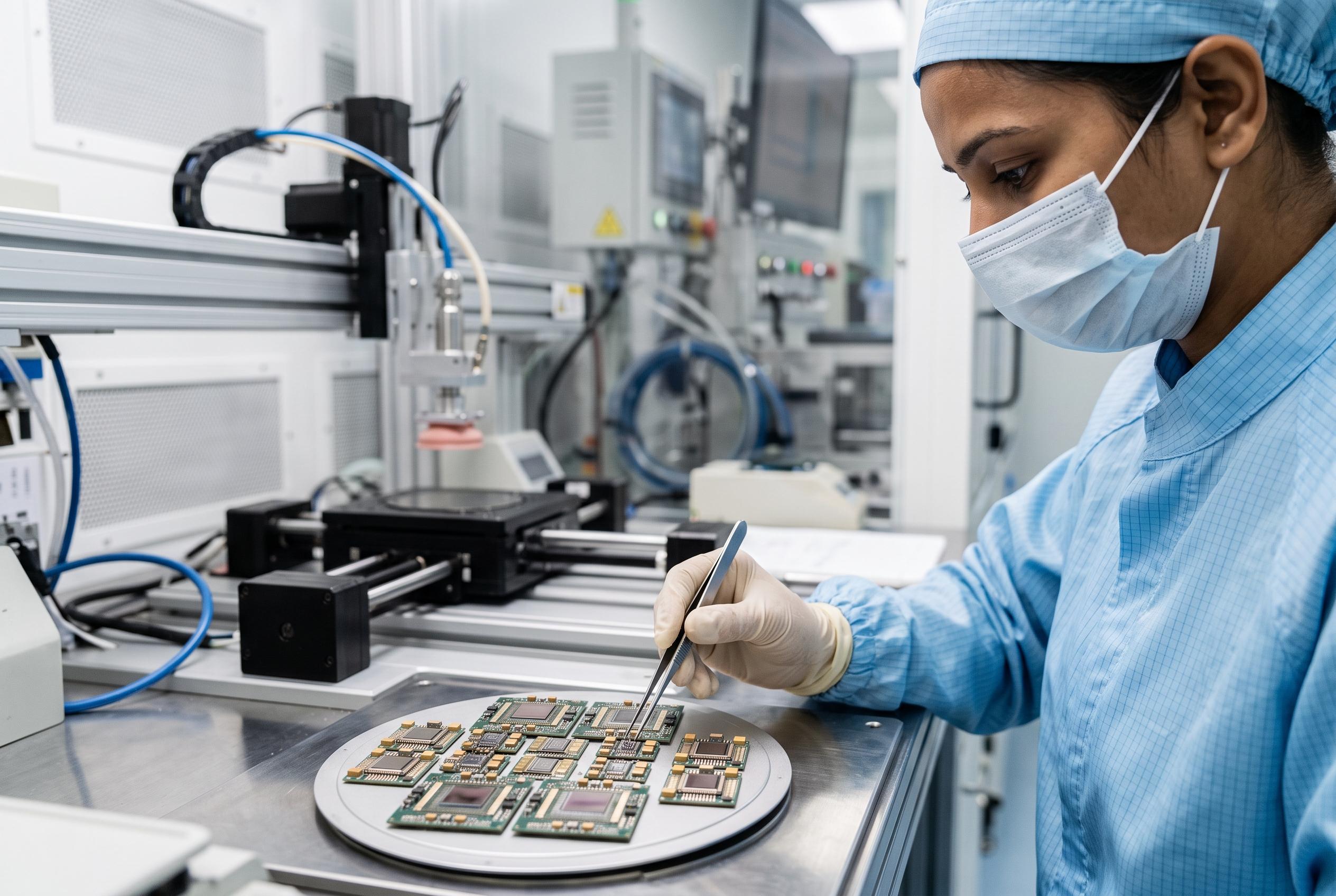

India is pivoting towards advanced packaging as a strategic move to strengthen its role in the global semiconductor supply chain, capitalising on lower entry barriers and rapid deployment potential amidst the evolving industry landscape.
Advanced packaging is emerging as one of the most realistic ways for India to gain a larger role in semiconductors, as the industry moves away from relying solely on ever-smaller transistors to improve chip performance. As Pareekh Jain, chief executive of EIIRTrend and Pareekh Consulting, told Business Today, chipmakers are increasingly combining multiple chiplets into a single package because shrinking transistors is becoming more difficult and more costly. That shift matters because advanced packaging can improve speed, cut power use and let companies mix chips made with different manufacturing processes.
The change is being driven most strongly by artificial intelligence and high-performance computing, where fast links between processors and high-bandwidth memory are essential. Jain said demand should stay strong as AI, data centres, automotive systems and other advanced applications lean more heavily on these technologies. That has already prompted large chipmakers and contract packaging specialists to pour money into new capacity, with companies such as TSMC, Intel, Samsung, Micron, ASE Group and Amkor Technology all expanding their advanced packaging footprint.
For India, the attraction is that packaging is far less capital-heavy than building a leading-edge fabrication plant, even though it is still far from cheap. Business Today reported that a mature-node fab can cost several billion dollars, while advanced packaging facilities can still require $2 billion to $8 billion and take close to three years to qualify for high-volume manufacturing. Sanchit Vir Gogia, chief analyst and chief executive of Greyhound Research, told the outlet that packaging offers “a wider capital ladder than fabrication, not an exemption from capital intensity”, pointing to large projects in Arizona and Malaysia as evidence that the segment remains expensive. Still, the entry barrier is lower, and the timeline to production is shorter.
That is one reason India’s new Semicon 2.0 push is paying more attention to advanced packaging. According to Business Standard, the scheme could help unlock more than ₹5 lakh crore in private and industry investment over the next five to seven years, while the broader policy framework is meant to cover fabrication, packaging, equipment, materials, design, research and training. PackNode reported that advanced packaging projects can receive support for up to 35% of eligible capital spending, including technologies such as 2.5D and 3D packaging, wafer-level chip-scale packaging and heterogeneous integration. The policy direction suggests New Delhi sees packaging as a quicker way to build depth in the domestic ecosystem.
Even so, the hard work lies in creating the surrounding industrial base. Jain said companies will still look for skilled engineers, reliable utilities, logistics, suppliers, customers and the ability to run at high yields, while India’s main weakness remains its limited local base for substrates, materials, equipment and experienced packaging talent. Gogia argued that India may not be late to the newest phase of chip manufacturing because chiplets, advanced integration and interposer technologies are still evolving, creating room for new entrants. That window, however, may not stay open for long. Grand View Research estimates the global advanced packaging market was worth $20.2 billion in 2024 and could reach $39.6 billion by 2030, underscoring how quickly the competitive landscape is tightening.
Disclaimer: This article is intended to inform and educate, not to recommend or endorse any financial product, investment or strategy. Please consider your own financial circumstances and seek professional advice where appropriate before making financial decisions.